AMD Ryzen Mobile 4000: Measuring Renoir’s Die Size
by Dr. Ian Cutress on January 14, 2020 9:00 AM EST- Posted in
- CPUs
- AMD
- Trade Shows
- Ryzen Mobile
- Renoir
- CES 2020
- Ryzen 4000
I’m pretty sure that the next time I go to a trade show where new silicon is being announced, the next tool I need in my backpack is a set of calipers in order to measure the die size. While die size doesn’t in of itself mean much as a number on its own, it is the end result of lots of hard work, focused co-design between silicon engineers and the semiconductor fabs, and ultimately there’s a fine balance between features, die size, performance, power, and at the end of the day, cost. With AMD showcasing the first x86-based 8-core CPU to move into the 15 W power envelope, finding out the die size is one of the elements of our investigation into how AMD has created its new Renoir / Ryzen Mobile 4000 product.
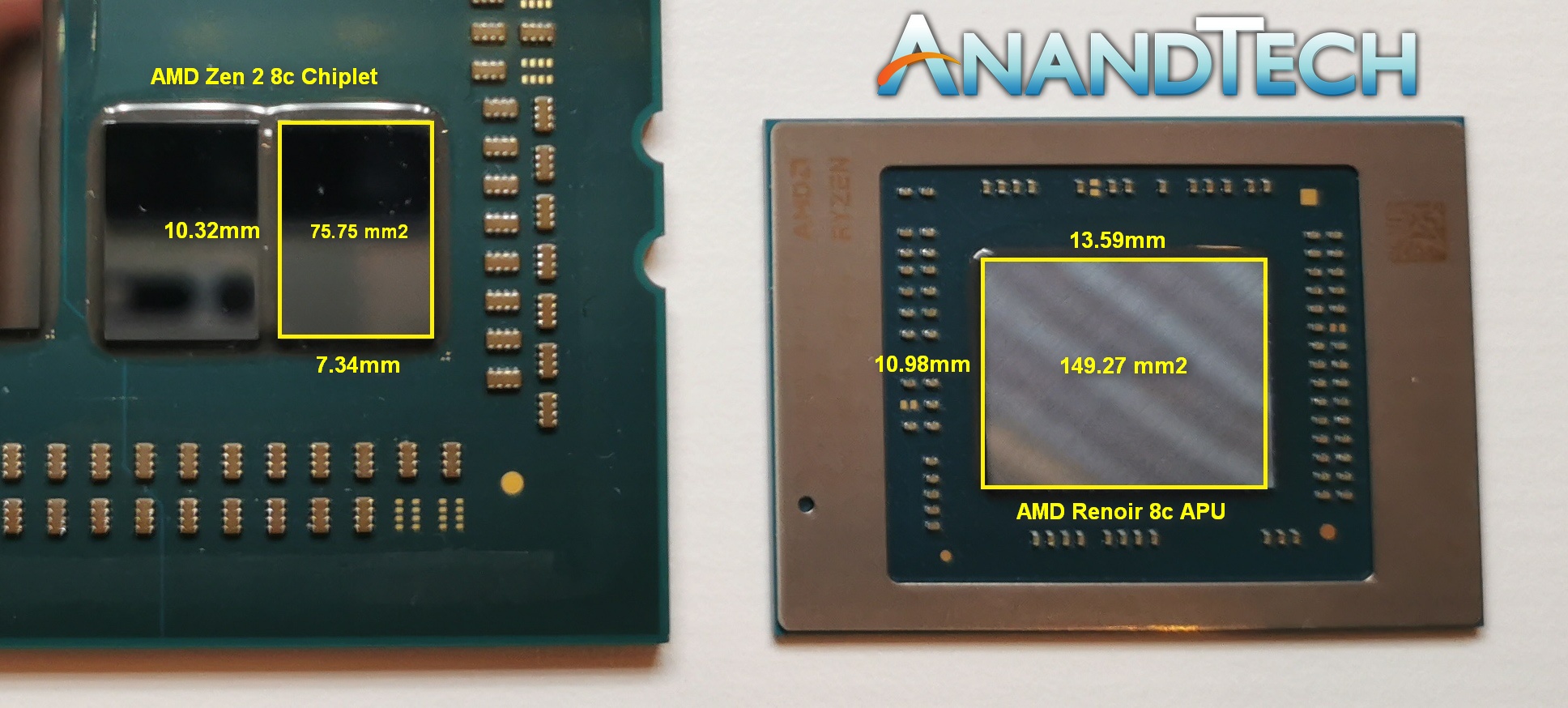
When I first saw the silicon, I wasn’t able to take pictures. Instead, I had to guess the size by manually placing it next to a 8-core Zen 2 chiplet from AMD’s monster 64-core Threadripper 3990X. We’ve known the die size for a while now, at 10.32 x 7.34 mm, or 75.75 mm2. My guess at the time that the new Renoir APU was almost exactly double the Zen 2 chiplet, and I mean it was scary how close to double the size it was. At the time of the announcement of Ryzen Mobile 4000, I had stated in our article that I estimated 150 mm2 for the die size. Turns out, I wasn’t too far wrong.
This image is not to scale.
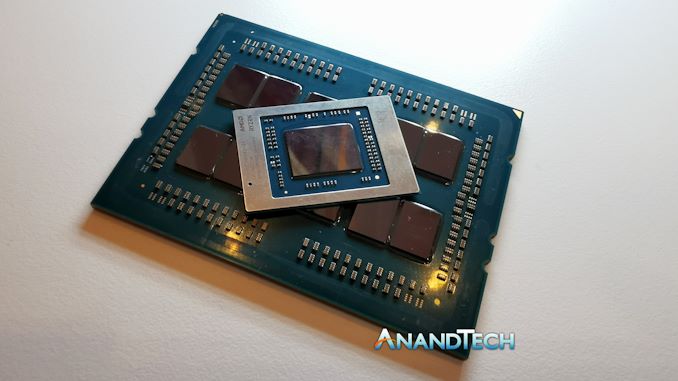
Later at CES, I went up to the AMD booth and this time they were more than happy for me to take photographs of the new silicon. The 3990X was also there, so I could place the two side by side and get a reasonable reference photograph on which to do calculations. This is the point of the event where I should have remembered to bring calipers! Taking photographs of chips is actually quite hard, making sure you get them lined up perfectly to get the same perspective, but also having enough light to get clear defined silicon edges.
In our picture, the Renoir chiplet you may notice is very slightly angled to the camera, which we’ve compensated for in our measurements.
With that in mind, here are our numbers.
The Zen 2 chiplet on the left, measures 10.32 mm by 7.34 mm, which is a ratio of 1.406 to 1.
In our image, the chiplet measured 265 pixels by 189 pixels, which is a ratio of 1.402 to 1.
In our image, the Renoir SoC measured 282 pixels by 350 pixels, which is a ratio of 0.806 to 1.
If we take the corresponding pixel dimensions, that gives us 10.98 mm by 13.59 mm, a ratio of 0.808 to 1.
This means that the die size of an eight-core Renoir APU with eight 2nd Gen Vega compute units, according to our calculations, 149.27 mm2.
| Die Sizes | ||||||
| AnandTech | x | y | Die Size | Process | Cores | EUs/ CUs |
| AMD Zen 2 Chiplet | 10.32 | 7.34 | 75.75 mm2 | TSMC N7 | 8 | - |
| Intel Ice Lake | 11.44 | 10.71 | 122.52 mm2 | Intel 10 | 4 | 64 |
| Intel Tiger Lake | 13.64 | 10.71 | 146.10 mm2 | Intel 10+ | 4 | 96 |
| AMD Picasso | 19.21 | 10.92 | 209.78 mm2 | GF 12 | 4 | 11 |
| AMD Renoir APU | 13.59 | 10.98 | 149.22 mm2 | TSMC N7 | 8 | 8 |
That’s pretty close to my 150 mm2 estimate, and I’ve also spoken to a few trusted individuals who have been tracking Zen 2 die structure sizes and graphics structure sizes, and they came out very similar, within 1mm2 or so.
At 149.27 mm2, assuming that AMD is achieving the same defect ratio on the silicon as reported by TSMC for the standard N7 process (0.09 defects per cm2), the process yield should be around 90%. Obviously that doesn’t take into account manufacturing for yield, or the distribution of the power/frequency of the chips within a wafer, but it’s still rather impressive.
Before AMD announced this new chip, there was a good deal of speculation as to how AMD would build it: either four cores with more graphics, or with eight cores and graphics only a little better. One factor of that was the die size: at 200 mm2, one would have expected AMD to definitely use eight cores. For sub 125 mm2, in order to maintain GPU performance, perhaps a quad-core design only have been suitable. However, AMD is claiming a great win here: eight Zen 2 cores, with frequencies at 1.8-4.3 GHz at 15 W, and despite fewer graphics compute units (down from 11 to 8), a higher per-compute unit performance claim of +56% means that performance is actually higher. All just shy of 150 mm2.
We are living in the future. I can’t wait for more.
It's worth noting that AMD's official number for the Zen 2 die size is 74 mm2. This is derived from the floorplan of the chip, which during manufacturing has additional space added to ensure clean die seperation between adjacent die prints. Ultimately what we get as the consumer is that seperation lane (known as a scribe lane) from one side of the die to the other, which is just slightly bigger than the floor plan that AMD supplies to the fabrication plant / TSMC. With calipers, what we get is that additional space, which is above AMD's quoted size.


103 Comments
View All Comments
milli - Tuesday, January 21, 2020 - link
You're not capable of reading comprehensively.Korguz - Tuesday, January 21, 2020 - link
oh.. and i take it you think you can ?? come on.. sounds to me like you are one of those " its ok if intel does it, but if amd does it.. then its unfair " type of people..Korguz - Tuesday, January 21, 2020 - link
further.. you also didnt fully explain why you think its unfair.... how is comparing base frequency to base frequency unfair ?? like i said.. on desktop.. the comparison has been intels higher clocks to amds lower clocks..is that fair ?? intel cant really get much higher clocks on these chips..Korguz - Saturday, February 15, 2020 - link
milli, yea thought so.. no other way to prove your point...twtech - Sunday, April 12, 2020 - link
Well, I think the average frequency under load is far more important than either base or max frequency.Not saying this is the case for any specific CPU, but if one CPU were to say, average halfway between min and max, while the other normally stays above 70% of max boost, there's a real difference there even if on paper they appear to share the same frequency range.
Namisecond - Wednesday, January 22, 2020 - link
But these aren't desktop CPUs with just 200mhz turbo boosts. These are mobile chips with huge turbo ranges.Thud2 - Sunday, February 9, 2020 - link
Korgus, I agree with your sentiment but the thing you're doing with the periods (...) is called an ellipses https://www.merriam-webster.com/dictionary/ellipsi... And it's meant to denote intentionally missing text. I think you're doing it do indicate a dramatic pause? You don't have to do that because your point is valid and it has a negative effect on the appearance of your comment to the reader.Namisecond - Wednesday, January 22, 2020 - link
Because you'll never see the base frequencies in operation of either? They'll jump around from between their dormant state speeds all the way up to max turbo until you reach thermal saturation, then it'll jump around even more. Sure, I could throw an ice-water liquid cooling loop on either, put them on mains power and tell them to TDP-up well past their 15W thermal spec and throw some massive server or content creation looped workload on them, but that's not what they were meant for.The base clock speed is a lie, for both camps.
Namisecond - Wednesday, January 22, 2020 - link
From what I've seen, Intel U mobile CPUs seem to have a base clock frequency of 800mhz no matter what the documentation states. It jumps around from there to max turbo speeds. ;pIrata - Thursday, January 16, 2020 - link
And this is the top 15W Ice Lake model vs. the bottom end Renoir...and the 8C 16T 4800 U still has a higher base clock (1.8 Ghz) and a higher turbo...Of course, we'll still have to wait for the first reviews of Renoir in a - hopefully - properly built and configured laptop to see how it does in real life (clocks, power consumption in idle, light load and heavy load).