2nm
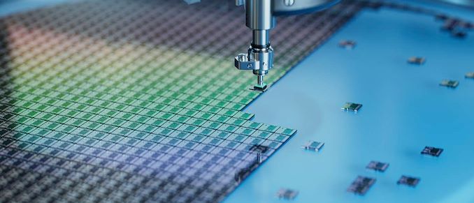
One of the core challenges that Rapidus will face when it kicks off volume production of chips on its 2nm-class process technology in 2027 is lining up customers. With Intel, Samsung, and TSMC all slated to offer their own 2nm-class nodes by that time, Rapidus will need some kind of advantage to attract customers away from its more established rivals. To that end, the company thinks they've found their edge: fully automated packaging that will allow for shorter chip lead times than manned packaging operations. In an interview with Nikkei, Rapidus' president, Atsuyoshi Koike, outlined the company's vision to use advanced packaging as a competitive edge for the new fab. The Hokkaido facility, which is currently under construction and is expecting to begin equipment installation...

TSMC Shares More Info on 2nm: New MIM Capacitor and Backside PDN Detailed
TSMC has revealed some additional details about its upcoming N2 and N2P process technology at its European Technology Symposium 2023. Both production nodes are being developed with high-performance computing...
15 by Anton Shilov on 5/31/2023
Samsung Foundry Vows to Surpass TSMC Within Five Years
The head of Samsung's semiconductor unit acknowledged last week that the company's current mass production, leading-edge process technologies are a couple of years behind TSMC's most advanced production nodes...
18 by Anton Shilov on 5/8/2023
TSMC Outlines 2nm Plans: N2P Brings Backside Power Delivery in 2026, N2X Added To Roadmap
At its 2023 North American Technology Symposium today, TSMC has disclosed additional details about its plans for its forthcoming N2 2nm-class production nodes in 2025 – 2026 and beyond...
38 by Anton Shilov on 4/26/2023
GlobalFoundries Sues IBM Over Sharing Leading-Edge Chip IP with Intel, Rapidus
The relationship between GlobalFoundries and IBM has been rocky in recent years. Among other things, Big Blue has previously sued GF, seeking damages for abruptly stopping the development of...
10 by Anton Shilov on 4/20/2023
Synopsys Intros AI-Powered EDA Suite to Accelerate Chip Design and Cut Costs
Synopsys has introduced the industry's first full-stack AI-powered suite of electronic design automation tools that covers all stages of chip design, from architecture to design and implementation to manufacturing...
12 by Anton Shilov on 3/30/2023
NVIDIA's cuLitho to Speed Up Computational Lithography for 2nm and Beyond
Production of chips using leading-edge process technologies requires more compute power than ever. To address requirements of 2nm nodes and beyond, NVIDIA is rolling out its cuLitho software library...
31 by Anton Shilov on 3/27/2023
Samsung Foundry Outlines Roadmap Through 2027: 1.4 nm Node, 3x More Capacity
Samsung outlined its foundry business roadmap for the next five years at its Foundry Forum event last week. The company plans to introduce its next generation fabrication technologies in...
14 by Anton Shilov on 10/10/2022
Samsung's $15 Billion R&D Complex to Overcome Limits of Semiconductor Scaling
Samsung on Friday broke ground for a new semiconductor research and development complex which will design new fabrication processes for memory and logic, as well as conduct fundamental research...
26 by Anton Shilov on 8/19/2022
TSMC: N2 To Start With Just GAAFETs, Add Backside Power Delivery Later
When TSMC initially introduced its N2 (2 nm class) process technology earlier this month, the company outlined how the new node would be built on the back of two...
16 by Anton Shilov on 6/29/2022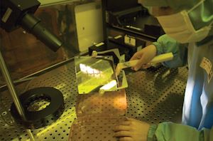
TSMC Unveils N2 Process Node: Nanosheet-based GAAFETs Bring Significant Benefits In 2025
At its 2022 Technology Symposium, TSMC formally unveiled its N2 (2 nm class) fabrication technology, which is slated to go into production some time in 2025 and will be...
24 by Anton Shilov on 6/16/2022
TSMC Roadmap Update: N3E in 2024, N2 in 2026, Major Changes Incoming
Taiwan Semiconductor Manufacturing Co. has solid plans for the next few years, but the foundry's manufacturing technology design cycles are getting longer. As a result, to address all of...
21 by Anton Shilov on 4/22/2022
TSMC Roadmap Update: 3nm in Q1 2023, 3nm Enhanced in 2024, 2nm in 2025
TSMC has introduced a brand-new manufacturing technology roughly every two years over the past decade. Yet as the complexity of developing new fabrication processes is compounding, it is getting...
32 by Anton Shilov on 10/18/2021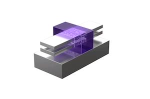
Samsung Foundry: 2nm Silicon in 2025
One of the key semiconductor technologies beyond 3D FinFET transistors are Gate-All-Around transistors, which show promise to help extend the ability to drive processors and components to higher performance...
29 by Dr. Ian Cutress on 10/6/2021
IBM Creates First 2nm Chip
Every decade is the decade that tests the limits of Moore’s Law, and this decade is no different. With the arrival of Extreme Ultra Violet (EUV) technology, the intricacies...
118 by Dr. Ian Cutress on 5/6/2021
TSMC to Spend $100B on Fabs and R&D Over Next Three Years: 2nm, Arizona Fab & More
TSMC this week has announced plans to spend $100 billion on new production facilities as well as R&D over the next three years. The world's largest contract maker of...
45 by Anton Shilov on 4/2/2021
Intel’s Manufacturing Roadmap from 2019 to 2029: Back Porting, 7nm, 5nm, 3nm, 2nm, and 1.4 nm
One of the interesting disclosures here at the IEEE International Electron Devices Meeting (IEDM) has been around new and upcoming process node technologies. Almost every session so far this...
138 by Dr. Ian Cutress on 12/11/2019


