NVIDIA Blackwell Architecture and B200/B100 Accelerators Announced: Going Bigger With Smaller Data
by Ryan Smith on March 18, 2024 5:00 PM EST
Already solidly in the driver’s seat of the generative AI accelerator market at this time, NVIDIA has long made it clear that the company isn’t about to slow down and check out the view. Instead, NVIDIA intends to continue iterating along its multi-generational product roadmap for GPUs and accelerators, to leverage its early advantage and stay ahead of its ever-growing coterie of competitors in the accelerator market. So while NVIDIA’s ridiculously popular H100/H200/GH200 series of accelerators are already the hottest ticket in Silicon Valley, it’s already time to talk about the next generation accelerator architecture to feed NVIDIA’s AI ambitions: Blackwell.
Amidst the backdrop of the first in-person GTC in 5 years – NVIDIA hasn’t held one of these since Volta was in vouge – NVIDIA CEO Jensen Huang is taking the stage to announce a slate of new enterprise products and technologies that the company has been hard at work on over the last few years. But none of these announcements are as eye-catching as NVIDIA’s server chip announcements, as it’s the Hopper architecture GH100 chip and NVIDIA’s deep software stack running on top of it that have blown the lid off of the AI accelerator industry, and have made NVIDIA the third most valuable company in the world.
But the one catch to making a groundbreaking product in the tech industry is that you need to do it again. So all eyes are on Blackwell, the next generation NVIDIA accelerator architecture that is set to launch later in 2024.
Named after Dr. David Harold Blackwell, an American statistics and mathematics pioneer, who, among other things, wrote the first Bayesian statistics textbook, the Blackwell architecture is once again NVIDIA doubling down on many of the company’s trademark architectural designs, looking to find ways to work smarter and work harder in order to boost the performance of their all-important datacenter/HPC accelerators. NVIDIA has a very good thing going with Hopper (and Ampere before it), and at a high level, Blackwell aims to bring more of the same, but with more features, more flexibility, and more transistors.
As I wrote back during the Hopper launch, “NVIDIA has developed a very solid playbook for how to tackle the server GPU industry. On the hardware side of matters that essentially boils down to correctly identifying current and future trends as well as customer needs in high performance accelerators, investing in the hardware needed to handle those workloads at great speeds, and then optimizing the heck out of all of it.” And that mentality has not changed for Blackwell. NVIDIA has improved every aspect of their chip design from performance to memory bandwidth, and each and every element is targeted at improving performance in a specific workload/scenario or removing a bottleneck to scalability. And, once again, NVIDIA is continuing to find more ways to less work altogether.
Ahead of today’s keynote (which by the time you’re reading this, should still be going on), NVIDIA offered the press a limited pre-briefing on the Blackwell architecture and the first chip to implement it. I say “limited” because there are a number of key specifications the company is not revealing ahead of the keynote, and even the name of the GPU itself is unclear; NVDIA just calls it the “Blackwell GPU”. But here is a rundown of what we know so far about the heart of the next generation of NVIDIA accelerators.
| NVIDIA Flagship Accelerator Specification Comparison | |||||
| B200 | H100 | A100 (80GB) | |||
| FP32 CUDA Cores | A Whole Lot | 16896 | 6912 | ||
| Tensor Cores | As Many As Possible | 528 | 432 | ||
| Boost Clock | To The Moon | 1.98GHz | 1.41GHz | ||
| Memory Clock | 8Gbps HBM3E | 5.23Gbps HBM3 | 3.2Gbps HBM2e | ||
| Memory Bus Width | 2x 4096-bit | 5120-bit | 5120-bit | ||
| Memory Bandwidth | 8TB/sec | 3.35TB/sec | 2TB/sec | ||
| VRAM | 192GB (2x 96GB) |
80GB | 80GB | ||
| FP32 Vector | ? TFLOPS | 67 TFLOPS | 19.5 TFLOPS | ||
| FP64 Vector | ? TFLOPS | 34 TFLOPS | 9.7 TFLOPS (1/2 FP32 rate) |
||
| FP4 Tensor | 9 PFLOPS | N/A | N/A | ||
| INT8/FP8 Tensor | 4500 T(FL)OPS | 1980 TOPS | 624 TOPS | ||
| FP16 Tensor | 2250 TFLOPS | 990 TFLOPS | 312 TFLOPS | ||
| TF32 Tensor | 1100 TFLOPS | 495 TFLOPS | 156 TFLOPS | ||
| FP64 Tensor | 40 TFLOPS | 67 TFLOPS | 19.5 TFLOPS | ||
| Interconnect | NVLink 5 18 Links (1800GB/sec) |
NVLink 4 18 Links (900GB/sec) |
NVLink 3 12 Links (600GB/sec) |
||
| GPU | "Blackwell GPU" | GH100 (814mm2) |
GA100 (826mm2) |
||
| Transistor Count | 208B (2x10⁴B) | 80B | 54.2B | ||
| TDP | 1000W | 700W | 400W | ||
| Manufacturing Process | TSMC 4NP | TSMC 4N | TSMC 7N | ||
| Interface | SXM | SXM5 | SXM4 | ||
| Architecture | Blackwell | Hopper | Ampere | ||
Tensor throughput figures for dense/non-sparse operations, unless otherwise noted
The first thing to note is that the Blackwell GPU is going to be big. Literally. The B200 modules that it will go into will feature two GPU dies on a single package. That’s right, NVIDIA has finally gone chiplet with their flagship accelerator. While they are not disclosing the size of the individual dies, we’re told that they are “reticle-sized” dies, which should put them somewhere over 800mm2 each. The GH100 die itself was already approaching TSMC’s 4nm reticle limits, so there’s very little room for NVIDIA to grow here – at least without staying within a single die.
Curiously, despite these die space constraints, NVIDIA is not using a TSMC 3nm-class node for Blackwell. Technically they are using a new node – TSMC 4NP – but this is just a higher performing version of the 4N node used for the GH100 GPU. So for the first time in ages, NVIDIA is not getting to tap the performance and density advantages of a major new node. This means virtually all of Blackwell’s efficiency gains have to come from architectural efficiency, while a mix of that efficiency and the sheer size of scaling-out will deliver Blackwell’s overall performance gains.
Despite sticking to a 4nm-class node, NVIDIA has been able to squeeze more transistors into a single die. The transistor count for the complete accelerator stands at 208B, or 104B transistors per die. GH100 was 80B transistors, so each B100 die has about 30% more transistors overall, a modest gain by historical standards. Which in turn is why we’re seeing NVIDIA employ more dies for their complete GPU.
For their first multi-die chip, NVIDIA is intent on skipping the awkward “two accelerators on one chip” phase, and moving directly on to having the entire accelerator behave as a single chip. According to NVIDIA, the two dies operate as “one unified CUDA GPU”, offering full performance with no compromises. Key to that is the high bandwidth I/O link between the dies, which NVIDIA terms NV-High Bandwidth Interface (NV-HBI), and offers 10TB/second of bandwidth. Presumably that’s in aggregate, meaning the dies can send 5TB/second in each direction simultaneously.
What hasn’t been detailed thus far is the construction of this link – whether NVIDIA is relying on Chip-on-Wafer-on-Substrate (CoWoS) throughout, using a base die strategy (AMD MI300), or if they’re relying on a separate local interposer just for linking up the two dies (ala Apple’s UltraFusion). Either way, this is significantly more bandwidth than any other two-chip bridge solution we’ve seen thus far, which means a whole lot of pins are in play.
On Blackwell accelerators, each die is being paired with 4 stacks of HBM3E memory, for a total of 8 stacks altogether, forming an effective memory bus width of 8192-bits. One of the constraining factors in all AI accelerators has been memory capacity (not to undersell the need for bandwidth as well), so being able to place down more stacks is huge in improving the accelerator’s local memory capacity. Altogether, the Blackwell GPU offers (up to) 192GB of HBM3E, or 24GB/stack, which is identical to the 24GB/stack capacity of H200 (and 50% more memory than the original 16GB/stack H100).
According to NVIDIA, the chip has an aggregate HBM memory bandwidth of 8TB/second, which works out to 1TB/second per stack – or a data rate of 8Gbps/pin. As we’ve noted in our previous HBM3E coverage, the memory is ultimately designed to go to 9.2Gbps/pin or better, but we often see NVIDIA play things a bit conservatively on clockspeeds for their server accelerators. Either way, this is almost 2.4x the memory bandwidth of the H100 (or 66% more than the H200), so NVIDIA is seeing a significant increase in bandwidth.
Finally, the TDP for this generation is also once again going up. With NVIDIA still on a 4nm-class node, and now packing over twice as many transistors into a single Blackwell GPU, there’s nowhere for TDPs to go except up. The B200 is a 1000W module, up from 700W for the H100. B200 machines can apparently still be air cooled, but it goes without saying that NVIDIA is expecting liquid cooling to be used more than ever, both out of necessity and for cost reasons. Meanwhile, for existing hardware installations, NVIDIA will also be releasing a lower-tier B100 accelerator with a 700W TDP, making it drop-in compatible with H100 systems.
Overall, compared to H100 at the cluster level, NVIDIA is targeting a 4x increase in training performance, and an even more massive 30x increase in inference performance, all the while doing so with 25x greater energy efficiency. We’ll cover some of the technologies behind this as we go, and more about how NVIDIA intends to accomplish this will undoubtedly be revealed as part of the keynote.
But the most interesting takeaway from those goals is the interference performance increase. NVIDIA currently rules the roost on training, but inference is a much wider and more competitive market. However, once these large models are trained, even more compute resources will be needed to execute them, and NVIDIA doesn’t want to be left out there. But that means finding a way to take (and keep) a convincing lead in a far more cutthroat market, so NVIDIA has their work cut out for them.
The Three Flavors of Blackwell: GB200, B200, and B100
NVIDIA will initially be producing three accelerators based on the Blackwell GPU.
| NVIDIA Blackwell Accelerator Flavors | |||||
| GB200 | B200 | B100 | |||
| Type | Grace Blackwell Superchip | Discrete Accelerator | Discrete Accelerator | ||
| Memory Clock | 8Gbps HBM3E | 8Gbps HBM3E | 8Gbps HBM3E | ||
| Memory Bus Width | 2x2x4096-bit | 2x4096-bit | 2x4096-bit | ||
| Memory Bandwidth | 2x8TB/sec | 8TB/sec | 8TB/sec | ||
| VRAM | 384GB (2x2x96GB) |
192GB (2x96GB) |
192GB (2x96GB) |
||
| FP4 Dense Tensor | 20 PFLOPS | 9 PFLOPS | 7 PFLOPS | ||
| INT8/FP8 Dense Tensor | 10 P(FL)OPS | 4.5 P(FL)OPS | 3.5 P(FL)OPS | ||
| FP16 Dense Tensor | 5 PFLOPS | 2.2 PFLOPS | 1.8 PFLOPS | ||
| TF32 Dense Tensor | 2.5 PFLOPS | 1.1 PFLOPS | 0.9 PFLOPS | ||
| FP64 Dense Tensor | 90 TFLOPS | 40 TFLOPS | 30 TFLOPS | ||
| Interconnects | 2x NVLink 5 (1800GB/sec) 2x PCIe 6.0 (256GB/sec) |
NVLink 5 (1800GB/sec) PCIe 6.0 (256GB/sec) |
NVLink 5 1800GB/sec) PCIe 6.0 (256GB/sec) |
||
| GPU | 2x "Blackwell GPU" | "Blackwell GPU" | "Blackwell GPU"GPU | ||
| GPU Transistor Count | 416B (2x2x104B) | 208B (2x10⁴B) | 208B (2x10⁴B) | ||
| TDP | 2700W | 1000W | 700W | ||
| Manufacturing Process | TSMC 4NP | TSMC 4NP | TSMC 4NP | ||
| Interface | Superchip | SXM-Next? | SXM-Next? | ||
| Architecture | Grace + Blackwell | Blackwell | Blackwell | ||
The flagship standalone accelerator is the B200, which with a TDP of 1000 Watts, is in a category all its own. This part is not drop-in compatible with existing H100 systems, and instead, new systems will be built around it.
Interestingly, despite this being the fastest of the traditional accelerators that NVIDIA will offer, this is not a peak-performance Blackwell configuration. B200 is still about 10% slower than what the fastest Blackwell product can achieve.
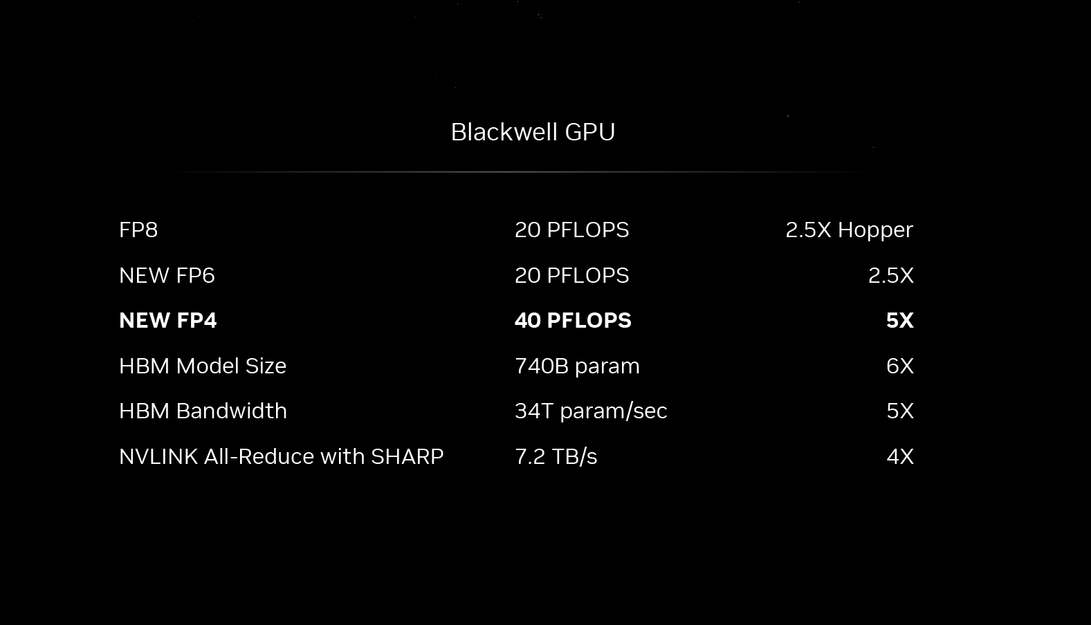
And what is that peak-performance product? The Grace Blackwell Superchip, GB200. Comprised of two Blackwell GPUs and a 72-core Grace CPU, GB200 is getting the fastest Blackwell GPUs of all. This is the only configuration with Blackwell GPUs that can hit 20 PFLOPS of sparse FP4 computational performance per GPU, for example. And, of course, with two Blackwell GPUs on a single superchip, the total throughput for the superchip is twice that, or 40 PFLOPS FP4.
As we don’t have any detailed specifications on the Blackwell GPU, it’s not clear here whether this is just a clockspeed difference, or if GB200 is getting a GPU configuration with more enabled tensor cores overall. But either way, if you want the best of Blackwell, you’ll need to buy it in the form of a GB200 Superchip, and the Grace that comes with it.
The power cost of GB200 is extensive, however. With 2 GPUs and a high-performance CPU on-board, GB200 modules can run at up to 2700 Watts, 2.7x the peak configurable TDP of the Grace Hopper 200 (GH200). Assuming a 300W TDP for the Grace CPU itself, this puts the TDP of the Blackwell GPUs in this configuration at a blistering 1200W TDP each. Ultimately, TDPs are somewhat arbitrary (you can usually go farther up the voltage/frequency curve a bit more for a lot more power), but broadly speaking, Blackwell’s most significant performance gains are coming at a cost of significantly higher power consumption, as well.
But for those customers who can’t afford a higher power budget, there is NVIDIA’s final Blackwell accelerator SKU: B100. HGX B100 boards are designed to be drop-in compatible with HGX H100 boards, operating at the same per-GPU TDP of 700 Watts. With the lowest TDP, this is the lowest-performing Blackwell accelerator variation, rated to deliver about 78% of B200’s compute performance. But compared to the H100 GPUs it would replace, B100 is slated to offer roughly 80% more computational throughput at iso-precision. And, of course, B100 gets access to faster and larger quantities of HBM3E memory.
At this time, NVIDIA has not announced pricing for any Blackwell configurations. The first Blackwell-based accelerators are set to ship later this year, but the company is not providing any guidance on which of the Blackwell flavors it will be (or if it will be all of them).
Second-Generation Transformer Engine: Even Lower Precisions
One of NVIDIA’s big wins with Hopper, architecturally speaking, was their decision to optimize their architecture for transformer-type models with the inclusion of specialized hardware – which NVIDIA calls their Transformer Engine. By taking advantage of the fact that transformers don’t need to process all of their weighs and parameters at a high precision (FP16), NVIDIA added support for mixing those operations with lower precision (FP8) operations to cut down on memory needs and improve throughput. This is a decision that paid off very handsomely when GPT-3/ChatGPT took off later in 2022, and the rest is history.
For their second generation transformer engine, then, NVIDIA is going to limbo even lower. Blackwell will be able to handle number formats down to FP4 precision – yes, a floating point number format with just 16 states – with an eye towards using the very-low precision format for inference. And for workloads where FP4 offers a bit too little precision, NVIDIA is also adding support for FP6 precision. FP6 doesn’t offer any compute performance advantages over FP8 – it essentially still goes through NVIDIA’s tensor cores as an FP8 operation – but it still offers memory pressure and bandwidth advantages thanks to the 25% smaller data sizes. LLM inference in general remains constrained by the memory capacity of those accelerators, so there’s a good deal of pressure to keep memory usage down with inference.
Meanwhile, on the training side of matters, NVIDIA is eyeing doing more training at FP8, versus BF16/FP16 as used today. This again keeps compute throughput high and memory consumption low. But what precision is used in LLM training is ultimately out of NVIDIA’s hands and up to developers, who need to optimize their models to work at these low precisions.
On that note, transformers have shown an interesting ability to handle lower precision formats without losing too much in the way of accuracy. But FP4 is quite low, to say the least. So absent further information, I am extremely curious how NVIDIA and its users intend to hit their accuracy needs with such a low data precision, as FP4 being useful for inference would seem to be what will make or break Blackwell as an inference platform.
In any case, NVIDIA is expecting a single Blackwell-based GPU to be able to offer up to 10 PetaFLOPS of FP8 performance with sparsity, or 5 PFLOPS with dense matrices. This is about 2.5x H100’s rate – and an even more absurd 20 PFLOPS of FP4 performance for inference. H100 doesn’t even benefit from FP4, so compared to its minimum FP8 data size, B200 should offer a 5x increase in raw inference throughput when FP4 can be used.
And assuming NVIDIA’s compute performance ratios remain unchanged from H100, with FP16 performance being half of FP8, and scaling down from there, B200 stands to be a very potent chip at higher precisions as well. Though at least for AI uses, clearly the goal is to try to get away with the lowest precision possible.
At the other end of the spectrum, what also remains undisclosed ahead of the keynote address is FP64 tensor performance. NVIDIA has offered FP64 tensor capabilities since their Ampere architecture, albeit at a much reduced rate compared to lower precisions. This is of little use for the vast majority of AI workloads, but is beneficial for HPC workloads. So I am curious to see what NVIDIA has planned here – if B200 will have much in the way of HPC chops, or if NVIDIA intends to go all-in on low precision AI.
NVLink 5: 1.8TB/second of Chip-to-Chip I/O Bandwidth, Multi-Rack Domain Scalability
Next to throwing down more tensor cores and more memory bandwidth, the third critical ingredient for accelerator performance from a hardware standpoint is interconnect bandwidth. NVIDIA is very proud of what they’ve accomplished over the last decade with their proprietary NVLink interconnect system, and they are continuing to iterate on that for Blackwell, both in regards to bandwidth and scalability. Especially in light of the need to network a large number of systems together to train the largest of LLMs in a timely fashion – and to put together a memory pool big enough to hold them – NVLink is a critical element in the design and success of NVIDIA’s accelerators.
With Blackwell comes the fifth generation of NVLink, which for the sake of simplicity we’re dubbing NVLink 5.
| NVLink Specification Comparison | |||||
| NVLink 5 | NVLink 4 | NVLink 3 | |||
| Signaling Rate | 200 Gbps | 100 Gbps | 50 Gbps | ||
| Lanes/Link | 2 | 2 | 4 | ||
| Bandwidth/Direction/Link | 50 GB/sec | 25 GB/sec | 25 GB/sec | ||
| Total Bandwidth/Link | 100 GB/sec | 50 GB/sec | 50 GB/sec | ||
| Links/Chip | 18 (Blackwell) |
18 (GH100) |
12 (GA100) |
||
| Bandwidth/Chip | 1800 GB/sec | 900 GB/sec | 600 GB/sec | ||
| PCIe Connectivity | PCIe 6.0 x16 | PCIe 5.0 x16 | PCIe 4.0 x16 | ||
Taking a look at the specifications disclosed thus far, at a high level, NVIDIA has doubled NVLink’s bandwidth from 900GB/second per GPU to 1800GB/second per GPU. Compared to previous generation products, this is the biggest jump in NVLink bandwidth in the last few years, as the 2022 Hopper architecture only offered a 50% gen-on-gen improvement in NVLink bandwidth.
Notably here, NVIDIA has doubled the amount of interconnect bandwidth at the same time as they’ve doubled the number of dies on a GPU, so the amount of data flowing into each die has not changed. But with the two dies needing to work together as a single processor, the total amount of data to be consumed (and to be shuffled around) has increased significantly.
More interestingly, perhaps, is that under the hood the number of NVLinks per GPU has not changed; GH100 Hopper’s NVLink capacity was 18 links, and Blackwell GPU’s NVLink capacity is also 18 links. So all of the bandwidth gains with NVLink 5 are coming from a higher signaling rate of 200Gbps for each high-speed pair within a link. This is consistent with the last few generations of NVLink, which has doubled the signaling rate with each iteration.
Otherwise, with the number of links being held constant from NVLink 4, the local chip topology options are essentially unchanged. NVIDIA’s HGX H100 designs have coalesced around 4 and 8-way setups, and HGX B200/B100 setups are going to be the same. Which doesn’t means that NVIDIA doesn’t have ambitions to grow the number of GPUs in a NVLink domain, but it will be a the rack level instead of the node level.
And that brings us to NVIDIA’s other (literally) big silicon announcement of the show: the fifth-generation NVLink Switch. The counterpart to the on-die capabilities of NVLink, NVIDIA’s dedicated NVLink switch chips are responsible for both single-node communications, and wiring up multiple nodes together within a rack. Even before NVIDIA picked up networking specialist firm Mellanox, the company was already offering switched GPU networking via NVLink switches.
This is breaking news. Additional details to follow


50 Comments
View All Comments
mode_13h - Thursday, March 21, 2024 - link
> Just having two dies is an improvement but feels like a baby step from what it could've been.Which is I'm sure why you bashed AMD for EPYC supporting only 2P scalability, right?
Sometimes, scaling to 2P is enough. Who says there'd have been room for more compute dies on half an SXM board? Also, once you go beyond 2 dies, maybe latency and bandwidth bottlenecks become too significant for the thing to continue presenting to software as one device.
There are complexities it seems you're just trying to wish away, for the sake of some imagined benefit that might not exist. Reply
Kevin G - Wednesday, March 27, 2024 - link
I have actually been critical of AMD sticking to dual socket support with Genoa. While a bit odd, the connectivity is there for three socket without sacrificing latency and only a hit to bandwidth. Quad socket would require some compromises but for the memory capacity hungry tasks, it'd be a win.The size of a SMX board is not hyper critical for nVidia. Making it longer is an easy trade off if they can pack in more compute in a rack.
As for scaling past 2 dies, you are correct that bandwidth and latency do impact scalability. The design does need to be mindful of the layout. Die-to-die traffic has to be prioritized, especially handling traffic where remote source and remote destination are passing through an intermediary die. Internal bandwidth needs to be higher than that of the local dies own memory bus. These are challenges for scalability but they are not insurmountable. One benefit nVidia has here is that they dictate the internal designs themselves: they know precisely how long it takes for data to move across the chip unlike a traditional dual socket system where board layout is handled by a 3rd party. In other words, scaling up in die count has a deterministic effect on latency.
There are other techniques that can be done to cut latency down: increasing the clock speeds and processing logic of command-and-control logic for coherency. For a chip whose execution units are running at ~2 Ghz max, a 4 Ghz bus and logic for cache coherency is within reason. And yes, the wire length does decrease with higher clock speed but signal repeaters exist for this reason. This grants the coherency logic more clock cycles to work and move data around with respect to the execution engines.
The main benefit of chiplets to is being able to obtain n-level scaling: a row of compute dies lined up with dedicated stacks of HBM flanking each compute die. Numerous compute units, lots of chip-to-chip bandwidth, large memory capacity and great memory bandwidth to let the design scale upward. Reply
name99 - Thursday, March 21, 2024 - link
"Per die performance only gets a mediocre increase but as a package this is a pretty respectable jump."This is simply not true, To hear the stories claimed above, using a Blackwell to train a large model would only require half as many GPUs (same number of underlying chips) and same amount of energy.
In fact It requires one quarter as many GPUs (ie each "chip" is 2x as effective), and one quarter as much energy...
And it's not like this is secret - Jensen specifically pointed this out.
Like I keep saying, peak FMAs is only a small part of the real-world performance of these chips and to obsess over it only shows ignorance. Reply
Dante Verizon - Saturday, March 23, 2024 - link
It should have nothing to do with the massive bandwidth and capacity of the HBM you now have available to power your very low-precision tasks.(FP4) LoL ReplyKevin G - Wednesday, March 27, 2024 - link
Looking at equal precision, The Blackwell package looks lo be roughly 2.25x that of the monolithic Hoppper. In other words, one Blackwell dies is roughly 1..25x that of Hopper which is faster but not that dramatic.The other chunk of performance gain is lowering precision via FP4. Reply
CiccioB - Tuesday, March 26, 2024 - link
You are oversimplify the scaling problem.You are not taking into account that each connection port to the close die requires a big transistor budget. And power too.
If you want that GPU to work as one single GPU with predictive behavior you have to consider the bandwidth of a single port shared between ALL dies as if die 1 wants the data present in the memory space of die 3 the data has to pass through the port connecting die 3 and 2 and then by the port connecting die 2 to 1. A single transmission uses double the bandwidth.
And it is worse if you have a fourth die.
You have to take into account the latency of such transmission which is obviously higher than one from die 2 to die 1 and even higher that from memory controllers in die 1.
Distributing data over NUMA architecture is not simple and the complexity raises as more dies are involved.
You have also to take into account the size of the underlaying interposer (which has a cost) and the energy required to transfer bunch of data between the interconnection ports.
You have to consider Ahmdal theorem as scaling is not free in terms of overhead (space, time and energy as said).
And at the end the total energy required by all those dies. Here we are already at 1200W for a single package. If you want to place another die and have the system scale to +50%, you will be consuming more than 1800W.
And those due would be bigger and to not have unused parts (unconnected ports, as you are not designing different dies for thiose at the extremes with a single port and those in the middle with two) you have to place 4 of then in a square structure thus coming with more than 2400W total consumption for a scale near 4x.
Losing only 20% of the calculation power due to darà movement overheads between dies (and the resulting loss of total available bandwidth) you end up with a bit more than 3x scaling for a 4x die architecture.
Consuming more than 4x by the way.
So you have a diminished return in terms of area, computation and power consumption, cost and thus margins.
If it were so easy to scale up with multi dies architectures we would already have packages as large as 1600cm² (40x40cm) with 32 memory channels.
But it is not, so just scaling up to 4 dies is already a challenge. Reply
nikaldro - Wednesday, March 20, 2024 - link
The node is N4P, not 4NP, and the previously used 4N was a 5nm class node Replymdriftmeyer - Friday, March 22, 2024 - link
People should really pay attention to patents granted. AMD forced Nvidia's hand early with the MI300 series and Nvidia comes out with Blackwell.I look forward to the excuses Nvidia fans make when the MI400 series is debuted. Most people could care less to read patents granted, but they should. It really shows how far ahead AMD is in the world of MCM designs now and down the road. Reply
name99 - Thursday, March 28, 2024 - link
Why don't you help us out?I do my part trying to collect and summarize Apple patents, how they fit together, and why they are valuable. You could do the same for AMD patents. Reply
webtasarimo - Wednesday, March 27, 2024 - link
With this development, I doubled my Nvidia shares. For now, we are at the beginning of new technologies that will come of age. I experienced Apple vision pro. Soon phones will be antiques. Artificial intelligence has evolved to an incredible size thanks to these chips. I'm so excited for the future Reply