YMTC Starts Volume Production of 64-Layer 3D NAND
by Anton Shilov on September 5, 2019 1:00 PM EST
Yangtze Memory Technologies Co. (YMTC) this week said that it had started volume production of its 64-layer 3D NAND memory that uses its proprietary Xtacking architecture. The bhips were developed entirely in China and will be used for SSDs as well as UFS storage.
YMTC’s 64-layer 3D TLC NAND device features a 256 Gb capacity, yet its interface speed is unknown. YMTC said that it would launch its own SSDs as well as UFS cards for embedded and mobile applications based on the new memory chips, but did not disclose any details about the said products or their availability timeframe.
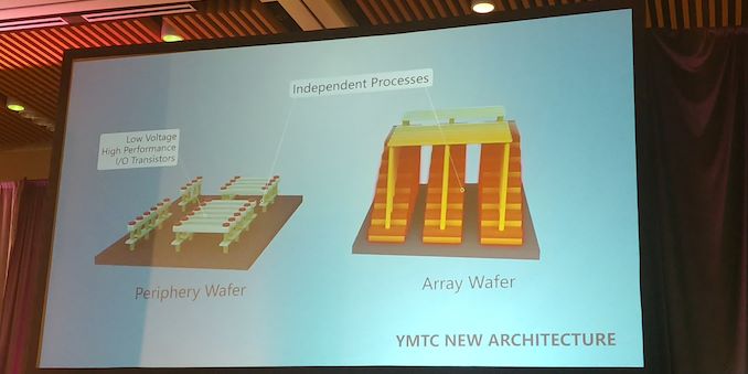
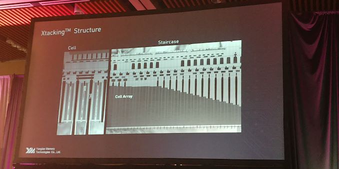
YMTC’s 3D NAND uses the company’s proprietary Xtacking architecture that is designed to enable very high I/O speeds and to some degree minimize die size. Traditionally, manufacturers of 3D NAND make memory array as well as NAND logic (address decoding, page buffers, etc.) on one wafer using the same process technology. By contrast, YMTC produces 3D NAND array and NAND logic on two separate wafers using different process technologies, and then bonds the two wafers together, connecting the memory arrays to the logic by metal vias using one additional process step. Making logic and I/O using an advanced process technology enables to increase I/O speed. Besides, the method places logic under the array, reducing die size of the actual device. YMTC says that Xtacking is not too expensive, though without revealing many details.
We have learned (but cannot verify) that a report suggests YMTC will output around 100,000 3D NAND wafers per month at XMC’s fab in Wuhan, China, in 2020. The same unconfirmed source states the output is expected to increase to 150,000 3D NAND wafers per month. This is quite a significant output, especially for China. While such production capacity will not immediately make YMTC a formidable rival to established 3D NAND makers globally, but it will certainly enable the company to gain some market share in China and this is exactly what it (and its parent Tsinghua Unigroup) wants.
Related Reading:
- Yangtze Memory Unveils Xtacking Architecture for 3D NAND: Up to 3 Gbps I/O
- Flash Memory Summit 2018, Yangtze Memory Technology Keynote Live Blog: Unleashing 3D NAND
- SK Hynix NAND Update: 3D NAND Output Cut, Slowdown Capacity Expansions
- Micron: Shipments of 3D QLC for SSDs Nearly Double QoQ as Wafer Starts Cut Again
- SK Hynix Launches 2nd Gen Enterprise SSD: 72-Layer 3D NAND & In-House Controller
- SK Hynix Launches 96-Layer 3D NAND and Discloses QLC Plans
- Samsung Shares SSD Roadmap for QLC NAND And 96-layer 3D NAND
Sources: Global Times, DigiTimes


3 Comments
View All Comments
azfacea - Thursday, September 5, 2019 - link
great news. the world needs more china in semiconductor and less frivilous lawsuits like the GF v TSMC recentlyGondalf - Thursday, September 12, 2019 - link
Likely Samsung do not agreed with you. This is the beginning of a big war in memory market.Both TSMC and GF are not involved much here.
Samsung want to penetrate hard in logic market in next ten years but with these aggressive Chineses around, I hardly believe they will have resources to realize this dream. All available money will be spent to try to defend the market share in memories.
otonieru - Thursday, January 9, 2020 - link
well, in the moment when almost every tech sites posting about the potential 40% increase of nand price this year, we need this more than anything. we need china to be able to supply nand, plenty enough and good enough it can nullify any supply gap in the market, and to prevent a price fixing practice potentially done by current player.