Samsung Starts Mass Production at V1: A Dedicated EUV Fab for 7nm, 6nm, 5nm, 4nm, 3nm Nodes
by Anton Shilov on February 20, 2020 1:00 PM EST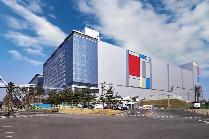
Samsung Foundry has started mass production of chips using its 6LPP and 7LPP manufacturing processes at its new V1 fab. The new facility employs one of the industry’s first production lines built from the ground up for technologies that heavily use EUV tools.
EUVL is a key enabler for Samsung’s next-generation leading-edge fabrication processes as it allows to reduce usage of multipatterning, and increases yields of chips architected for smaller technologies. Samsung currently uses EUVL equipment for its 6LPP and 7LPP nodes, and will expand its usage in future nodes such as 5LPE, 4LPE, 3GAE, and 3GAP processes.
| Advertised PPA Improvements of New Process Technologies Data announced by companies during conference calls, press briefings and in press releases |
||||||
| 7LPP vs 10LPE |
6LPP vs 7LPP |
5LPE vs 7LPP |
3GAE vs 7LPP |
|||
| Power | 50% | lower | 20% | 50% | ||
| Performance | 20% | ? | 10% | 35% | ||
| Area Reduction | 40% | ~9% | <20% | 40% | ||
Samsung Foundry’s 7LPP and 6LPP process technologies are used to make advanced mobile SoCs that will be shipped in Q1. The contract manufacturer of semiconductors does not disclose names of its client(s), but it is noteworthy that its 6LPP technology is not a part of its MPW (multi project wafer) shuttle program, which may indicate that the process is only available for Samsung itself and/or select customers who do not use MPWs.

Samsung’s 6LPP is a evolution of its 7LPP node that offers slightly higher (~10%) transistor density and lower power, but is compatible with, and can reuse IP initially developed for 7LPP. Furthermore, 6LPP supports smart structures for designers eager to invest in all-new IP, as well as multi diffusion break feature. Meanwhile, 5LPE promises to bring further advantages when it comes to power, performance, when compared to 6LPP.
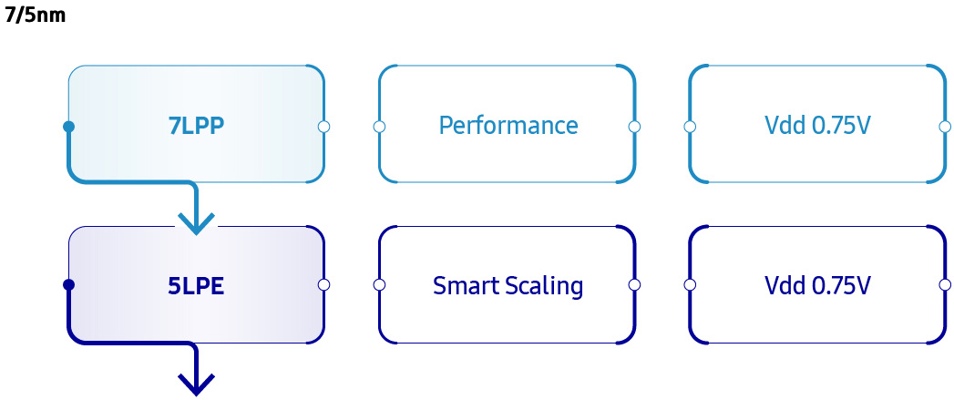
6LPP looks to be a limited offer node for select customers, whilst Samsung's focus in the future looks to be on its new 5LPE node.
| Global Manufacturing Sites of Samsung Foundry | ||||||||
| Name | 6-Line | S1 | S2 | S3 | S4 | V1 | ||
| Nodes | 180~65nm | 65~8nm | 65~11nm | 10nm~ | 65nm~ | 7nm~ | ||
| Location | Giheung, South Korea | Austin, Texas | Hwaseong, South Korea | |||||
| Wafer Size | 200 mm | 300 mm | ||||||
Samsung’s V1 fab is located in Hwaseong, Korea, adjacent to its S3 line, where Samsung started initial ramp of chips made using its 7LPP technology. The company began construction of V1 in February 2018, and initiated test wafer production in the second half of 2019. Samsung continues to ramp up its V1 fab now and says that by the end of the year its total capacity for EUV-enabled 7LPP and below nodes will be three times higher than it was in 2019. Meanwhile, cumulative investments in the V1 line will hit $6 billion by the end of 2020.

Related Reading:
- ASML Ramps Up EUV Scanners Production: 35 in 2020, Up to 50 in 2021
- EUV Demand is Up: EUV Device Manufacturer ASML Beats Sales Estimates
- Samsung Starts Mass Production of Chips Using Its 7nm EUV Process Tech
- Samsung Foundry Updates: 8LPU Added, EUVL on Track for HVM in 2019
- Samsung Completes Development of 5nm EUV Process Technology
Source: Samsung


29 Comments
View All Comments
Vitor - Thursday, February 20, 2020 - link
Intel: Wait, isn't that illegal?nandnandnand - Friday, February 21, 2020 - link
Samsung/TSMC: I will make it legal.ksec - Thursday, February 20, 2020 - link
Samsung Foundry doesn't really have a history to deliver on time, quality, and volume. They are surely working hard and investing a lot, ( especially from their NAND and DRAM branches ), but it remains to be seen whether they can really compete with TSMC.drexnx - Thursday, February 20, 2020 - link
huh? Apple fabbed there for yearsksec - Friday, February 21, 2020 - link
They were not leading edge.mercucu1111 - Friday, February 21, 2020 - link
Samsung leads in 14nm. And TSMC didn't have counterpart of 14LPE in 2015Q1. 16FF has same cell size, CPP, M2P of 20SoC.Samsung leads HKMG, 14nm, 10nm and EUV Process. Why do you think that sammy isn't cutting edge? It is very bad joke.
Eliadbu - Saturday, February 22, 2020 - link
I remmber when Apple fabed both with Samsung and TSMC, after reports came that chips fabed at Samsung draw more power than TSMC, they switched completely to TSMC year or couple of years later. If I'm not mistaken it was with Samsung 14nm vs TSMC 16nm. So no Samsung manufacturing process are not the lead nor their 14nm process. Other than dry facts of sizes there more details that may set one manufacturer process from another. Matter of fact their leading Logic fabs have fallen behind TSMC. Now they are in the game of catching up with competition and that why they decided to invest tens of billions USD each year for the next 10 years.mercucu1111 - Saturday, February 22, 2020 - link
https://pc.watch.impress.co.jp/img/pcw/docs/1209/9...https://pc.watch.impress.co.jp/img/pcw/docs/1209/9...
It's because 14LPE 9T has lesser cell size than TSMC's 7.5T One. So Die size of Sammy's A9 is much smaller. And In low clock, 14LPE comsumes power much lesser than 16FF.
http://drmola.com/files/attach/images/56517/226/04...
On the other hand, 16FF has advantage in high clock. So TSMC's A9 has advantage in CPU Stress test.
mercucu1111 - Saturday, February 22, 2020 - link
https://www.tomshardware.com/news/iphone-6s-a9-sam...In CPU Stress test. S.LSI's 14LPE consumes more power. But In General use, S.LSI's APL0898 has mare battery life perfomance. I'm using my phone for general use. Not an benchmarking machine that driving Geekbench 24/7. Talking 14LPE is inferior node than 16FF in CPU Stress test is very bad joke.
In your logic, TSMC 7FF is inferior than 14++ or 14+++ because they can reach more clock speed.
MASSAMKULABOX - Monday, February 24, 2020 - link
Wasnt their a similar thing with Qualcom Phone Socs? some drew a lot more power than others , especially made for the USA market?