TSMC Establishes Joint Venture to Build 12nm/16nm Fab in Europe
by Anton Shilov on August 8, 2023 8:23 AM EST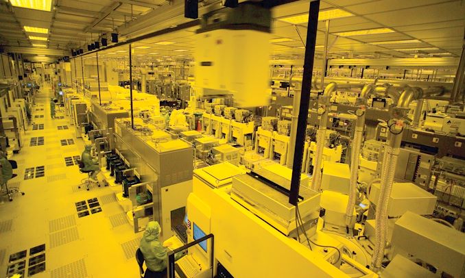
TSMC on Tuesday announced plans to establish a European Semiconductor Manufacturing Company (ESMC) joint venture with its partners Bosch, Infineon, and NXP to build a fab near Dresden, Germany. The new 300-mm fab will produce chips on TSMC's 28/22 nm and 16/12 nm-class process technologies, primarily for automotive and industrial sectors. As the project is planned under the European Chips Act framework, TSMC is set to get subsidies to build it.
The proposed ESMC fab will be located near Dresden, Germany, and is slated to have a monthly production capacity of 40,000 300mm wafer starts per month. The fab is set to use TSMC's 28 nm family of production nodes, which includes several specialty manufacturing technologies and a 22 nm low-power fabrication process with planar transistors and 16 nm and 12 nm production technologies featuring FinFETs. The fab, which TSMC will operate, will employ about 2,000 workers and engineers.
ESMC intends to start fab construction in the latter half of 2024 and start making its first products there by the end of 2027. As TSMC planned, the proposed fab will mainly serve automakers based in Germany and Austria, ensuring a steady supply of chips to these companies in the latter half of the decade.
"This investment in Dresden demonstrates TSMC's commitment to serving our customer's strategic capacity and technology needs, and we are excited at this opportunity to deepen our long-standing partnership with Bosch, Infineon, and NXP," said Dr. CC Wei, Chief Executive Officer of TSMC.
Meanwhile, since the fab will only make chips on mature 12/16 nm and 22/28 nm process technologies, automakers will still need to source advanced processors required for self-driving and sophisticated infotainment systems from TSMC's fabs in Taiwan and the U.S. Therefore, companies like Bosch, BMW, Infineon, Mercedes Benz Group, NXP, Stellantis, and Volkswagen Group will be able to get various microcontrollers and sensors from ESMC, their most advanced proprietary components that will define capabilities of their software-defined vehicles will be built in Taiwan or the USA by TSMC or Germany by Intel Foundry Services.
Yet, mature process technologies are required not only for automotive and industrial sectors, but also for various emerging applications that fall under the Internet-of-Things umbrella. These will benefit significantly from TSMC's low-power 22 nm production node and N12e process technology.
"Infineon will use the new capacity to serve the growing demand particularly of its European customers, especially in automotive and IoT," said Jochen Hanebeck, CEO of Infineon Technologies. "The advanced capabilities will provide a basis for developing innovative technologies, products and solutions to address the global challenges of decarbonization and digitalisation."
Financially, the venture is structured such that TSMC will have a 70% stake, with the remaining partners each holding a 10% equity stake. The collective investments for this initiative are forecasted to surpass €10 billion. ESMC is expected to get around €5 billion in subsidies under the Europen Chips Act and from the German government.
Source: TSMC


10 Comments
View All Comments
meacupla - Tuesday, August 8, 2023 - link
I can see this fab being successful, unlike that 2nm fab that is also planned for 2027 elsewhere.Arnulf - Tuesday, August 8, 2023 - link
So they are planning to go in GloFo's Fab 1 back yard and compete with them directly on automotive etc. production?name99 - Tuesday, August 8, 2023 - link
I'm guessing something like this was the only way to get the European Chips Act passed.France gets its fab in Crolles, run by GloFo, and Germany gets its fab in Dresden, run by TSMC.
Diogene7 - Tuesday, August 8, 2023 - link
In theory, would a chip design implemented on a 20A GAA-FET or below FPGA consume less power than the same chip design implemented on a 28nm ASIC ?As the 20A die would be much smaller than the 28nm ASIC, would it cost much more ?
I have difficulty understanding why bothering so much designing ASIC on 28nm / 40nm or upper node, and not nowadays (2023 / 2025) implement them using 20A (2nm) FPGA as it would be on a smaller die, and also it might be possible to update it afterwards ?
How much more expensive would it be at scale ?
I am not an expert, just trying to understand what are the challenges that prevents this to happen ?
ET - Tuesday, August 8, 2023 - link
As I understand it, the main issue isn't price but resilience. The larger process size is less susceptible to interference, so if reliability matters, it's better to use it. Also, less dense chips are easier to cool.But on the price front, yes, the denser chip will likely be more expensive. The technology required for 20A is much more expensive and the creation of such chips is harder and more expensive. An FPGA saves on the chip creation costs, but is a lot less efficient, so adds cost on that front.
It's worth noting that the density of "28nm" vs. "2nm" refers to logic density. A lot of the space on embedded chips is SRAM and flash, which don't scale nearly as well, as well as I/O. So basically the chip won't be much smaller, yet will be many times more expensive.
Diogene7 - Wednesday, August 9, 2023 - link
« The technology required for 20A is much more expensive and the creation of such chips is harder and more expensive ». —> If « transfering » as many 28nm or higher node ASIC designs to 2nm (20A) FPGA as possible would be done at high volume, it would maybe increase the 2nm FPGA volume manufacturing, and maybe help decrease the cost of 2nm FPGA.« An FPGA saves on the chip creation costs, but is a lot less efficient, so adds cost on that front » —> In terms of the overall chip energy consumption, I would think that 28nm or higher node ASIC design may consume a similar amount of energy as a 2nm (20A) less energy efficient FPGA thanks to that 2nm transistors consumes a lot less than 40nm transistors (even if there is a need of several 2nm transistors in an 2nm FPGA to do the same thing than a single one 40nm transistor in a 40nm ASIC design).
« A lot of the space on embedded chips is SRAM and flash, which don't scale nearly as well, as well as I/O« —> A new generation of FPGA could be using emerging Non Volatile Memory (NVM) like VG-SOT-MRAM that I think is smaller than current SRAM / Flash which would also help « shrinking » the design.
I unfortunately don’t have access to many detailed information to have a clear view of what would be all the trade-offs, but I am wondering if toward 2028, 2030, 2032 it would make much economical sense to manufacture ASIC designed on all older 28nm, 40nm,… nodes when, with new forthcoming innovations (MRAM, spintronic, carbon nanotubes,…) foundries may be able to offer reasonably priced competitive innovative FPGA on 2nm (20A) or below that could also be « updated » afterwards if necessary…
ET - Wednesday, August 9, 2023 - link
It's not just a matter of volume manufacturing in terms of demand. Manufacturing at 20A requires much larger machine that take a lot more power, are a lot more sensitive to dust, movement, ...Regarding forthcoming innovations, it will depend on their cost and availability. Currently MRAM is available at 28nm and is planned for 12/14nm. In the long run, who knows...
I still think that even in the long run, the newest processes will be busy making the newest high performance CPUs/GPUs/TPUs. Using them for smaller designs doesn't have any advantage that I can see. Sure, if we end up moving to a completely different paradigm, they might fit there, but they currently have the advantage of simple and cheap manufacturing, easy design and an end result which is good enough for the intended purpose.
Diogene7 - Wednesday, August 9, 2023 - link
Thanks very much for the feedback : As I szid, I am not an expert, so this is helpful.Santoval - Saturday, August 19, 2023 - link
Regarding leakage and interference aren't GAA-FETs meant to mitigate it compared to FinFETs?If GAA-FETs replaced an existing FinFET node without however making them smaller node for node they should be quite more resistant to leakage.
But they're also meant to increase transistor density, so they'll have tighter specs. Do you think they'll face a leakage issue already from their first gen?
Santoval - Saturday, August 19, 2023 - link
It would consume less power if it had the same clock.It would probably be harder to cool though due to the much higher thermal density, despite a lower TDP in total.
As for costs a 20A wafer would be far more expensive than a 28nm wafer.
The cost per die would be partly but not fully offset by the many more dies per wafer of the 20A node.
The final cost per die would depend on cost per wafer, yields and how much smaller the dies were compared to the mature node dies. As a general rule the more SRAM they have the worst they scale, since SRAM does not scale as much as logic (as ET noted).