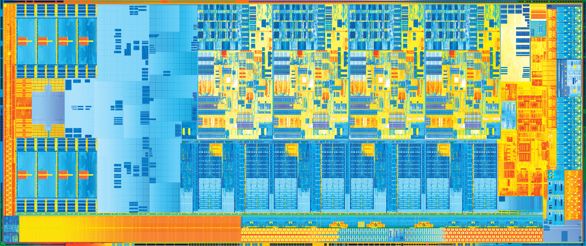
Dual Core/GT2 Ivy Bridge Die Measured: ~121mm^2
by Anand Lal Shimpi on May 31, 2012 2:25 PM EST- Posted in
- CPUs
- Intel
- Ivy Bridge
- Ultrabook
I mentioned Intel's desired secrecy around die sizes and transistor counts for the majority of the Ivy Bridge lineup in our 3470 review from this morning. While I can't count individual transistors in the Core i7-3517U that was in ASUS' Zenbook Prime UX21A we reviewed a week ago, I can measure its exposed die.
Mobile CPUs rarely feature integrated heatspreaders, giving us direct access to the back side of the processor die itself. The dual-core die looks very similar to the quad-core die, it's just not as long. Armed with a pair of digital calipers, I can get a good idea of the CPU's die area.
The die measures approximately 14.7mm x 8.2mm, covering 120.54mm^2 of area. That's roughly 75% of the die area of the quad-core/GT2 Ivy Bridge part:
| CPU Specification Comparison | ||||||||
| CPU | Manufacturing Process | CPU Cores | Transistor Count | Die Size | ||||
| Apple A5R2 | 32nm LP | 2 | ?? | 69mm2 | ||||
| Apple A5X | 45nm LP | 2 | ?? | 163mm2 | ||||
| AMD Bulldozer 8C | 32nm | 8 | 1.2B | 315mm2 | ||||
| Intel Ivy Bridge 2C (GT2) | 22nm | 2 | ?? | 121mm2 | ||||
| Intel Ivy Bridge 4C (GT2) | 22nm | 4 | 1.4B | 160mm2 | ||||
| Intel Sandy Bridge E (6C) | 32nm | 6 | 2.27B | 435mm2 | ||||
| Intel Sandy Bridge E (4C) | 32nm | 4 | 1.27B | 294mm2 | ||||
| Intel Sandy Bridge 4C | 32nm | 4 | 1.16B | 216mm2 | ||||
| Intel Lynnfield 4C | 45nm | 4 | 774M | 296mm2 | ||||
| Intel Sandy Bridge 2C (GT1) | 32nm | 2 | 504M | 131mm2 | ||||
| Intel Sandy Bridge 2C (GT2) | 32nm | 2 | 624M | 149mm2 | ||||
I included the two Apple SoCs to put Intel's 2C/GT2 die size in perspective. It's entirely possible to build very high performance smartphone/tablet class silicon given a modern enough manufacturing process. While I doubt we'll see anything this class in an iPad anytime soon, when we get to Broadwell (14nm Haswell shrink) the tablet market will be very interesting indeed. Haswell is expected to narrow the idle power consumption gap that separates ARM and big x86 silicon, while increasing die size at the high end. Broadwell will bring die area back in check with a move to 14nm.


18 Comments
View All Comments
sciwizam - Thursday, May 31, 2012 - link
Any idea on what the die sizes are for the S4, T3 or the Exynos 4?dagamer34 - Thursday, May 31, 2012 - link
Here's a comparison with a few other SoCs: http://www.anandtech.com/show/5688/apple-ipad-2012...What's surprising is that if Intel is selling chips at $100+ with this die size on a new process whereas a 160mm^2 die can be had for $20-25, then I think die size and cost aren't as tightly coupled as I previously thought (or Intel is charging a ton for its chips)
name99 - Thursday, May 31, 2012 - link
Or the upfront costs for(a) designing the chip
(b) designing the process
are phenomenal, and, even amortized over tens of millions of chips, add substantially to the cost of each chip...
it's also possible that the A5X was specifically designed to be fault tolerant ---- not in the most general sense, but in the sense that the large arrays (L2 cache and the GPU arrays) are wired up to allow for some fraction of defects.
Obviously Intel do the same thing, but if you're striving for maximal performance, you may be rather more constrained in how you can do this than at lower performance goals. Anyone have any real info on this?
iwod - Thursday, May 31, 2012 - link
Designing the Process doesn't count. Or you mean Designing "for" the process?Designing the Process count as a cost towards TSMC / Samsung, or the Fab Players.
I think dagamer34 is correct, the Cost of $30 in the case of Apple A5X ( it is actually estimated to be $25 range, but just bump it up for example ) already includes the cost of Fabbing it. Which means the Foundry Profits.
That also includes ARM and PowerVR Licenses Cost.
What we dont know is the R&D Apple put into their SoC, At 100Million Apple SoC per year that additional $5 would have pretty much cover that already.
If you consider that, Intel is making an additional MINIMUM of $70 per Chip profits Intel Gains.
Although Intel properly make a discount somewhere to gain Apple's order.
CeriseCogburn - Friday, June 1, 2012 - link
Just wanted to say good job getting that die size and good job posting it in proper form.JKflipflop98 - Saturday, June 2, 2012 - link
Uh, designing the process certainly does count. It's a very, very expensive procedure retooling and recalibrating process tools for a new product. Maybe ARM doesn't have to worry about that, but Intel certainly does.ShieTar - Friday, June 1, 2012 - link
The coupling between die size and cost is not really based on the price of the silicium. A 300 mm wafer will cost you a few hundred $, and will probably yield about 300 to 400 chips of 160 mm² size.What you have to take into consideration is the fact that your expensive lithography machine will illuminate one wafer in a certain amount of time, and the salaries and power cost that run up in that time need to be divided by the number of chips included in that wafer. Also the machine will not operate forever, so its buying cost needs to be divided by the number of chips produced in its expected operating time. Smaller chips means the machine-cost per chip goes down.
That means of course that the link between size and cost is only specific to one certain fab and process. It is clear that TSMC can offer 160 mm² in a 45nm-process significantly cheaper than INTEL can offer 160 mm² in the new 22 nm-process.
gplnpsb - Thursday, May 31, 2012 - link
Intel may not have watned to release the exact die sizes to the press, but the exact die dimensions are listed in the Volume 1 Datasheet for the Mobile 3rd Generation Intel Core Processor family. It is available here: http://www.intel.com/content/dam/www/public/us/en/...There are four desktop Ivy Bridge dies:
4C GT2 8MB L3 "Ivy Bridge-HE-4" 19.631x8.141mm = 159.816 mm2 (E-1 Stepping)
4C GT1 6MB L3"Ivy Bridge-HM-4" 17.349x7.656mm = 132.824 mm2 (N-0 Stepping)
2C GT2 4MB L3 "Ivy Bridge-H-2" 14.505x8.141mm = 118.085 mm2 (L-1 Stepping)
2C GT1 3MB L3 "Ivy Bridge-M-2" 12.223x7.656mm = 93.579 mm2 (P-0 Stepping)
I derived those figures from the Mechanical Package drawings on page 161 to 165 of the document I linked. The 4C GT1 die isn't listed in the database, but I derived it's dimensions by subtracting the difference in length between the GT1 and GT2 dual core dies and subtracting it from the 4C die. Logically the height would be the same as the GT1 dual core die. Its worth mentioning that if you check Intels MDDS database for the S-Spec codes of the desktop quad cores launched today (ie the i5 3470 SR0T8/QCBU) you will see they are mostly based on the 133 mm2 Ivy Bridge-HM-4 die.
If you check pages 14 and 15 of the Desktop specification update: http://www.intel.com/content/dam/www/public/us/en/... you will see that they are based on the N-0 stepping, not E1. It's worth mentioning that the GT2 dual core die is the L-1 stepping, and the GT1 dual core die is the P-0 stepping.
JarredWalton - Thursday, May 31, 2012 - link
+5 to you! ;-)What I find odd is that Intel *does* release this information, just not always in a clear, concise format. It's like certain sects as Anand calls them have decided people aren't going to figure it out if marketing doesn't tell us, but the Internet doesn't work like that.
Even with the above estimates, it's not like we really have a lot more to discuss. 4C GT2 is bigger than 4C GT1, which in turn is bigger than 2C GT2 and the smallest is 2C GT1. Shocking, right?
gplnpsb - Thursday, May 31, 2012 - link
Haha, quite right, its not exactly shocking. One interesting thing however is that Intel felt it worthwhile to spend a few million dollars creating separate masks for a 4C GT1 die. They never bothered to do that with Sandy Bridge. All quad core Sandy Bridge chips were based on the same 216 mm2 die.I guess the reasoning is that a hypothetical 4C GT1 Sandy Bridge would have been 193 mm2, reducing die size by only 11%. The 2C GT1 Sandy Bridge die was 14% smaller than the 2C GT2 die.
With Ivy Bridge, the 4C GT1 die is 17% smaller than the 4C GT2 die, and the 2C GT1 die is 20% smaller than the 2C GT2 die.
Presumably the HD 2500 Core i5 Ivy Bridge chips are going to be extremely popular with OEMs. If so, volumes will be high enough to ensure that a separate die significant improves Intel's profit margins.